


Industry
 Num:72
 See:1786
2021-06
10
Master these tips to make it easy for you to operate DC-DC circuits!
Concept and characteristics
concept
DC-DC refers to Direct Current power supply. A device that converts electrical energy from one voltage to another voltage in a direct current circuit. For example, one DC voltage (5.0V) can be converted to another DC voltage (1.5V or 12.0V) through a converter, we call this converter DC-DC converter, or called the switching power supply or switch regulator.
DC-DC converter is generally composed of control chip, inductor coil, diode, transistor, capacitor. When discussing the performance of DC-DC converter, it is impossible to judge the advantages and disadvantages of the control chip only. The characteristics of the components of the peripheral circuit and the wiring mode of the substrate can change the performance of the power circuit. Therefore, comprehensive judgment should be made.
DC - DC converter simplifies the use of the power supply circuit design, shorten the development cycle, achieve best indicator, etc., are widely used in power electronic, military, scientific research, industrial control equipment, communications equipment, instruments and meters, exchange equipment, access equipment, mobile communications, routers and other communications and industrial control, automotive electronics, aerospace and other fields. With the characteristics of high reliability and easy system upgrade, the application of power module is more and more widely. In addition, DC-DC converters are also widely used in mobile phones, MP3, digital cameras, portable media players and other products. It belongs to chopper circuit in the classification of circuit type.
characteristics
Its main feature is high efficiency: compared with the LDO of linear regulators, high efficiency is a significant advantage of DCDC. Usually the efficiency is more than 70%, and the high efficiency can reach more than 95%. The second is to adapt to a wide voltage range.
Modulation
1: PFM (Pulse Frequency Modulation Mode)
Switch pulse width is certain, by changing the pulse output frequency, so that the output voltage to achieve stability. PFM control type has the advantage of small power consumption even if it is used for a long time, especially when the load is small.
2: PWM (Pulse Width Modulation Mode)
The frequency of the switch pulse is fixed, and the output voltage is stable by changing the output width of the pulse. PWM control type has high efficiency and good output voltage ripple and noise.
B: In general, the performance differences of DC-DC converters using PFM and PWM modulation modes are as follows.
PWM frequency, PFM duty cycle selection method. PWM/PFM conversion type implements PFM control when small load, and automatically converts to PWM control when heavy load.
Architecture classification
Three common principles of architecture
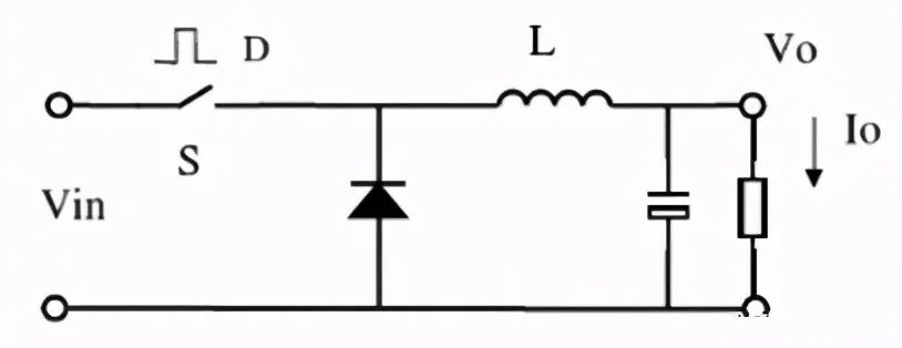
A, Buck (Buck type DC/DC converter)
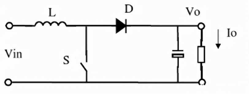
B, Boost (Boost DC/DC converter)
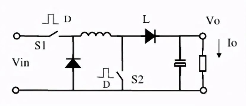
C, Buck-Boost (up and down voltage DC/DC converter)
Detailed explanation of the working principle of Buck circuit
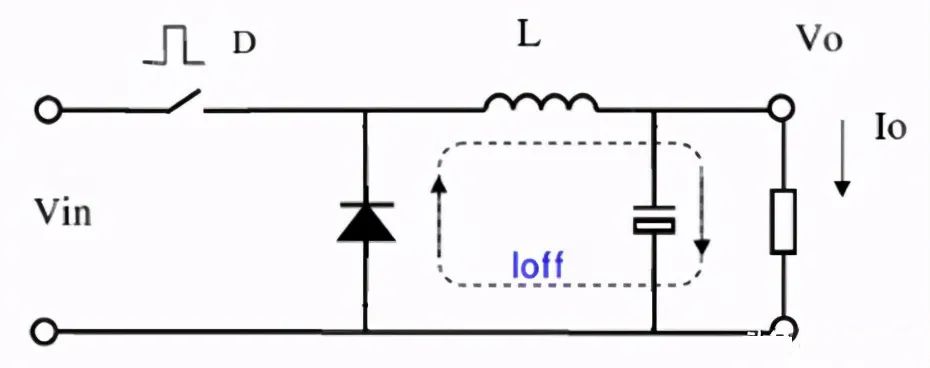
The principle of volt second balance: for an inductor in a stable state, the positive volt second product at both ends of the inductor is equal to the negative volt second product, that is, the volt second product at both ends of the inductor must be balanced within a switching period.
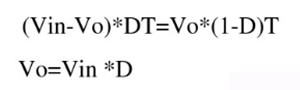
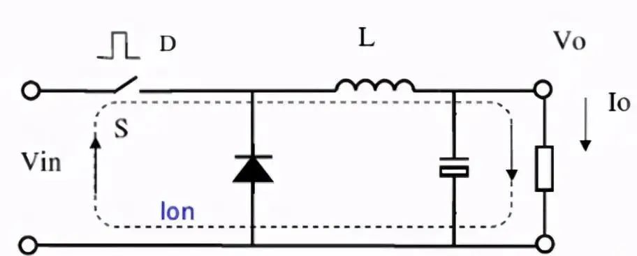
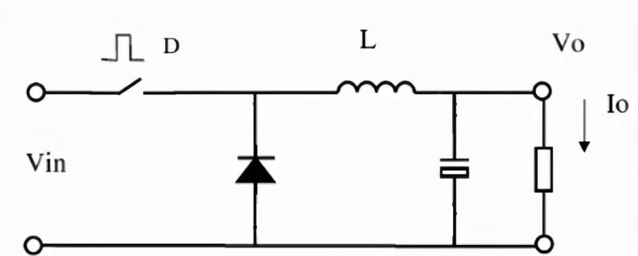
When the switch is on: the input voltage VIN is applied to the input of the LC filter, and the current on the inductor increases linearly with a fixed slope. The following figure:
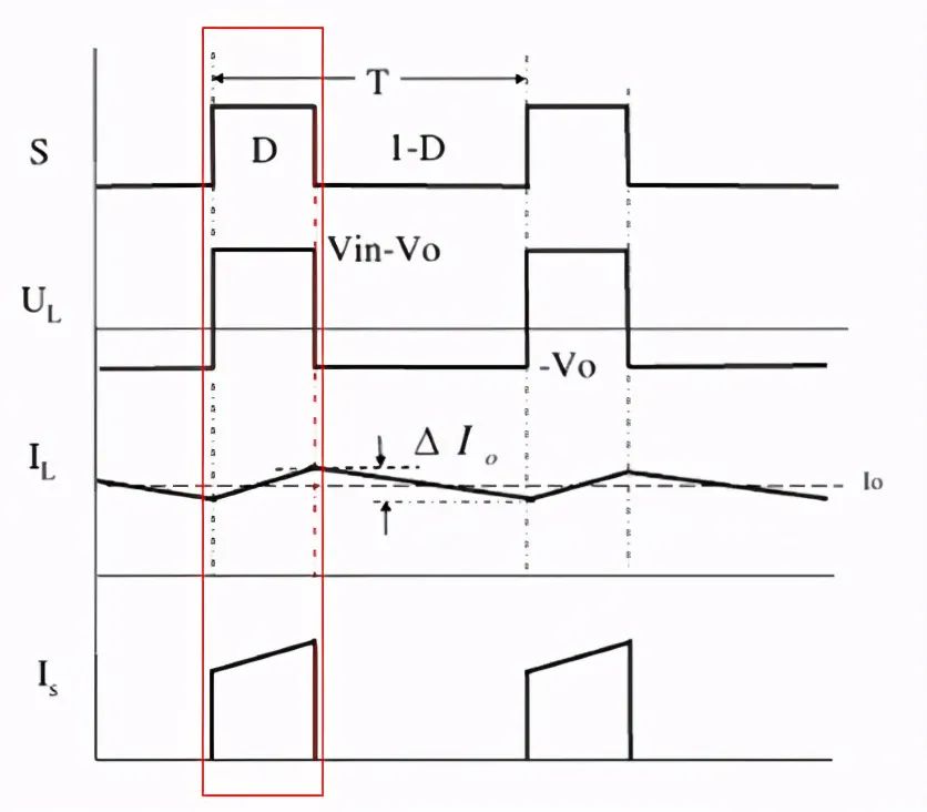
When the switch is off: since the current on the inductor cannot be switched off, the energy stored in the inductor is released to the load, and the inductor current continues through the diode. At this stage, the current waveform is a negative slope slope. The following figure:
Design skills and main technical parameter selection requirements
At least the following conditions should be considered in the design of DC-DC circuit:
A. Range of external input power supply voltage and output current.
B. Maximum output voltage, current and system power of DC-DC.
input/output voltage
The recommended operating voltage range of the device should be selected, and the actual voltage fluctuation range should be considered to ensure that the device specification is not exceeded.
Output current
The continuous output current capacity of the device is an important parameter, which should be taken into account when selecting, and some allowance should be retained.
The selection of this parameter should also evaluate the instantaneous peak current of the circuit and the heating situation, and comprehensively determine, and meet the requirements of derating.
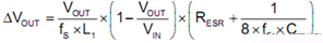
ripple
Ripple is an important parameter to measure the output voltage fluctuation of a circuit. The ripple of light load and heavy load should be paid attention to. Generally the ripple of light load is larger. Pay attention to whether the light load ripple will exceed the requirements in the case of nuclear power. Actual testing of various scenarios under load. Usually the oscilloscope 20M bandwidth is used for testing.
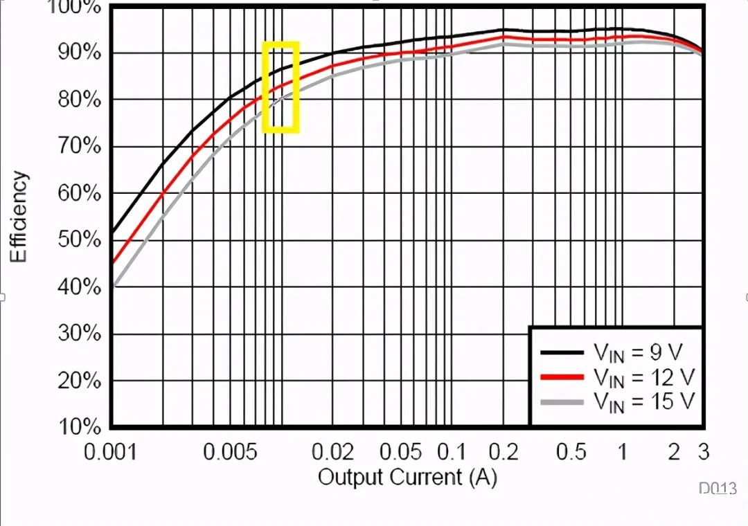
efficiency
Pay attention to both light and heavy loads. Light load will affect the standby power, heavy load affects the temperature rise. Usually see 12V input, 5V output under the efficiency of 10mA, generally more than 80%.
Transient response
Transient response characteristics reflect whether the system can adjust in time to ensure the stability of the output voltage when the load changes dramatically. Output voltage fluctuation is required to be as small as possible, generally according to the peak-to-peak value below 10% requirements.
In practice, the feedback capacitance should be selected according to the recommended value. The common values are between 22p and 120pF.
Switching frequency
The most commonly used switching frequency is more than 500kHz. High switching frequency 1.2m to 2M also have, due to the high frequency switch loss increase IC heat dissipation design is better, so mainly focused on 5V low-voltage input small current products. Switching frequency is related to the selection of inductors and capacitors, and other problems such as EMC and noise under light load are also related to it.
Feedback reference voltage and accuracy
The feedback voltage should be compared with the internal reference voltage and output different voltages with the external feedback divider resistor. The reference voltage of different products will be different, such as 0.6~0.8V, pay attention to adjust the feedback resistance when replacing.
The feedback resistance should be 1% precision, as long as the manufacturer recommended to choose, generally do not choose too large, so as not to affect the stability.
The accuracy of the reference voltage affects the output accuracy. The common accuracy is less than 2%, such as 1%~1.5%, and the cost of the product with high accuracy will be different. Choose according to need.
Linear stability and load stability
Linear stability reflects input voltage variation and output voltage stability. Load stability reflects the output voltage stability when the output load changes. The general requirement is 1%, the maximum should not exceed 3%.
EN level
EN High and low levels must meet device specifications. Some ICs must not exceed a specific voltage range. When the resistance voltage is divided, pay attention to meet the timely shutdown, and consider the maximum range of voltage fluctuation to meet.
For timing control, the pin will increase the capacitance for level regulation and shutdown discharge, as well as resistance to the ground.
Protection performance
There should be overcurrent protection OCP, overheat protection OTP, and protection after the disappearance of conditions can be self-recovery.
other
Soft start is required; Thermal resistance and packaging; The use temperature range should be able to cover high and low temperature.
General principles of device selection
Universality, a.
High cost performance
Easy to purchase long life cycle
Compatible and replaceable
Resource conservation
Derating
Easy to produce and normalize
Requirements for selection of peripheral devices
Input capacitance
To meet the requirements of voltage resistance and input ripple. General voltage requirements 1.5~2 times more than the input voltage. Note that the actual capacitance of the chip is reduced by dc voltage bias.
Output capacitance
To meet the requirements of voltage resistance and output ripple. General pressure requirements 1.5~2 times
The relationship between ripple and capacitance:
BST capacitance
Recommended values according to the specifications. Generally 0.1 uF uF - 1. The withstand voltage is generally higher than the input voltage.
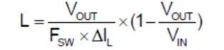
inductance
Different output voltages require different inductance. Note that temperature rise and saturation current should meet the allowance requirements, generally more than 1.2 times the maximum current (or the saturation current of the inductor must be greater than the maximum output current +0.5* inductor ripple current). A suitable inductance value L is usually chosen so that ΔIL accounts for 30% to 50% of the output current. Calculation formula:
VCC capacitor
According to the specifications of the requirements of the value, can not be reduced, also do not be too large, pay attention to pressure.
Feedback capacitance
According to the requirements of the specification, different chip manufacturers have different values, and different output voltage will also have different requirements.
07 Feedback resistance and EN sub-piezoelectric
Require value according to specification book, accuracy 1%.
VI.PCB design requirements
1. Input capacitance is placed near the input VIN and power PGND of the chip to reduce the existence of parasitic inductance, because the input current is discontinuous and the noise caused by parasitic inductance has a bad effect on the voltage withstand and logic unit of the chip. Capacitance ground end to increase the hole, reduce impedance.
2. The power loop should be as short and thick as possible to maintain a small loop area and less noise radiation. SW is a noise source that ensures the current while keeping the area as small as possible, away from sensitive and vulnerable locations. For example, the inductor is near the SW pin and away from the feedback line. The output capacitor is close to the inductor, the ground end increases the ground pass hole.
3. The VCC capacitor should be placed in the nearest layer between the VCC pin of the chip and the signal ground of the chip, and there should be no holes.
4.FB is the most sensitive and easily disturbed part of the chip, and is the most common cause of system instability.
1) The FB resistor connected to the FB pin may be short and placed close to the IC to reduce the coupling of noise; Under FB, the voltage divider is usually connected with signal ground AGNd;
2) Away from noise source, SW point, inductor, diode (asynchronous buck); FB routing package land;
3) FB with large current load should be taken at the far end of the load, and the feedback capacitor wiring should be taken nearby.
5. The capacitance of BST should be as short as possible, not too thin.
6 chip heat dissipation according to the design requirements, as far as possible in the bottom to increase the hole heat dissipation.
concept
DC-DC refers to Direct Current power supply. A device that converts electrical energy from one voltage to another voltage in a direct current circuit. For example, one DC voltage (5.0V) can be converted to another DC voltage (1.5V or 12.0V) through a converter, we call this converter DC-DC converter, or called the switching power supply or switch regulator.
DC-DC converter is generally composed of control chip, inductor coil, diode, transistor, capacitor. When discussing the performance of DC-DC converter, it is impossible to judge the advantages and disadvantages of the control chip only. The characteristics of the components of the peripheral circuit and the wiring mode of the substrate can change the performance of the power circuit. Therefore, comprehensive judgment should be made.
DC - DC converter simplifies the use of the power supply circuit design, shorten the development cycle, achieve best indicator, etc., are widely used in power electronic, military, scientific research, industrial control equipment, communications equipment, instruments and meters, exchange equipment, access equipment, mobile communications, routers and other communications and industrial control, automotive electronics, aerospace and other fields. With the characteristics of high reliability and easy system upgrade, the application of power module is more and more widely. In addition, DC-DC converters are also widely used in mobile phones, MP3, digital cameras, portable media players and other products. It belongs to chopper circuit in the classification of circuit type.
characteristics
Its main feature is high efficiency: compared with the LDO of linear regulators, high efficiency is a significant advantage of DCDC. Usually the efficiency is more than 70%, and the high efficiency can reach more than 95%. The second is to adapt to a wide voltage range.
Modulation
1: PFM (Pulse Frequency Modulation Mode)
Switch pulse width is certain, by changing the pulse output frequency, so that the output voltage to achieve stability. PFM control type has the advantage of small power consumption even if it is used for a long time, especially when the load is small.
2: PWM (Pulse Width Modulation Mode)
The frequency of the switch pulse is fixed, and the output voltage is stable by changing the output width of the pulse. PWM control type has high efficiency and good output voltage ripple and noise.
B: In general, the performance differences of DC-DC converters using PFM and PWM modulation modes are as follows.
PWM frequency, PFM duty cycle selection method. PWM/PFM conversion type implements PFM control when small load, and automatically converts to PWM control when heavy load.
Architecture classification
Three common principles of architecture
A, Buck (Buck type DC/DC converter)
B, Boost (Boost DC/DC converter)
C, Buck-Boost (up and down voltage DC/DC converter)
Detailed explanation of the working principle of Buck circuit
The principle of volt second balance: for an inductor in a stable state, the positive volt second product at both ends of the inductor is equal to the negative volt second product, that is, the volt second product at both ends of the inductor must be balanced within a switching period.
When the switch is on: the input voltage VIN is applied to the input of the LC filter, and the current on the inductor increases linearly with a fixed slope. The following figure:
When the switch is off: since the current on the inductor cannot be switched off, the energy stored in the inductor is released to the load, and the inductor current continues through the diode. At this stage, the current waveform is a negative slope slope. The following figure:
Design skills and main technical parameter selection requirements
At least the following conditions should be considered in the design of DC-DC circuit:
A. Range of external input power supply voltage and output current.
B. Maximum output voltage, current and system power of DC-DC.
input/output voltage
The recommended operating voltage range of the device should be selected, and the actual voltage fluctuation range should be considered to ensure that the device specification is not exceeded.
Output current
The continuous output current capacity of the device is an important parameter, which should be taken into account when selecting, and some allowance should be retained.
The selection of this parameter should also evaluate the instantaneous peak current of the circuit and the heating situation, and comprehensively determine, and meet the requirements of derating.
ripple
Ripple is an important parameter to measure the output voltage fluctuation of a circuit. The ripple of light load and heavy load should be paid attention to. Generally the ripple of light load is larger. Pay attention to whether the light load ripple will exceed the requirements in the case of nuclear power. Actual testing of various scenarios under load. Usually the oscilloscope 20M bandwidth is used for testing.
efficiency
Pay attention to both light and heavy loads. Light load will affect the standby power, heavy load affects the temperature rise. Usually see 12V input, 5V output under the efficiency of 10mA, generally more than 80%.
Transient response
Transient response characteristics reflect whether the system can adjust in time to ensure the stability of the output voltage when the load changes dramatically. Output voltage fluctuation is required to be as small as possible, generally according to the peak-to-peak value below 10% requirements.
In practice, the feedback capacitance should be selected according to the recommended value. The common values are between 22p and 120pF.
Switching frequency
The most commonly used switching frequency is more than 500kHz. High switching frequency 1.2m to 2M also have, due to the high frequency switch loss increase IC heat dissipation design is better, so mainly focused on 5V low-voltage input small current products. Switching frequency is related to the selection of inductors and capacitors, and other problems such as EMC and noise under light load are also related to it.
Feedback reference voltage and accuracy
The feedback voltage should be compared with the internal reference voltage and output different voltages with the external feedback divider resistor. The reference voltage of different products will be different, such as 0.6~0.8V, pay attention to adjust the feedback resistance when replacing.
The feedback resistance should be 1% precision, as long as the manufacturer recommended to choose, generally do not choose too large, so as not to affect the stability.
The accuracy of the reference voltage affects the output accuracy. The common accuracy is less than 2%, such as 1%~1.5%, and the cost of the product with high accuracy will be different. Choose according to need.
Linear stability and load stability
Linear stability reflects input voltage variation and output voltage stability. Load stability reflects the output voltage stability when the output load changes. The general requirement is 1%, the maximum should not exceed 3%.
EN level
EN High and low levels must meet device specifications. Some ICs must not exceed a specific voltage range. When the resistance voltage is divided, pay attention to meet the timely shutdown, and consider the maximum range of voltage fluctuation to meet.
For timing control, the pin will increase the capacitance for level regulation and shutdown discharge, as well as resistance to the ground.
Protection performance
There should be overcurrent protection OCP, overheat protection OTP, and protection after the disappearance of conditions can be self-recovery.
other
Soft start is required; Thermal resistance and packaging; The use temperature range should be able to cover high and low temperature.
General principles of device selection
Universality, a.
High cost performance
Easy to purchase long life cycle
Compatible and replaceable
Resource conservation
Derating
Easy to produce and normalize
Requirements for selection of peripheral devices
Input capacitance
To meet the requirements of voltage resistance and input ripple. General voltage requirements 1.5~2 times more than the input voltage. Note that the actual capacitance of the chip is reduced by dc voltage bias.
Output capacitance
To meet the requirements of voltage resistance and output ripple. General pressure requirements 1.5~2 times
The relationship between ripple and capacitance:
BST capacitance
Recommended values according to the specifications. Generally 0.1 uF uF - 1. The withstand voltage is generally higher than the input voltage.
inductance
Different output voltages require different inductance. Note that temperature rise and saturation current should meet the allowance requirements, generally more than 1.2 times the maximum current (or the saturation current of the inductor must be greater than the maximum output current +0.5* inductor ripple current). A suitable inductance value L is usually chosen so that ΔIL accounts for 30% to 50% of the output current. Calculation formula:
VCC capacitor
According to the specifications of the requirements of the value, can not be reduced, also do not be too large, pay attention to pressure.
Feedback capacitance
According to the requirements of the specification, different chip manufacturers have different values, and different output voltage will also have different requirements.
07 Feedback resistance and EN sub-piezoelectric
Require value according to specification book, accuracy 1%.
VI.PCB design requirements
1. Input capacitance is placed near the input VIN and power PGND of the chip to reduce the existence of parasitic inductance, because the input current is discontinuous and the noise caused by parasitic inductance has a bad effect on the voltage withstand and logic unit of the chip. Capacitance ground end to increase the hole, reduce impedance.
2. The power loop should be as short and thick as possible to maintain a small loop area and less noise radiation. SW is a noise source that ensures the current while keeping the area as small as possible, away from sensitive and vulnerable locations. For example, the inductor is near the SW pin and away from the feedback line. The output capacitor is close to the inductor, the ground end increases the ground pass hole.
3. The VCC capacitor should be placed in the nearest layer between the VCC pin of the chip and the signal ground of the chip, and there should be no holes.
4.FB is the most sensitive and easily disturbed part of the chip, and is the most common cause of system instability.
1) The FB resistor connected to the FB pin may be short and placed close to the IC to reduce the coupling of noise; Under FB, the voltage divider is usually connected with signal ground AGNd;
2) Away from noise source, SW point, inductor, diode (asynchronous buck); FB routing package land;
3) FB with large current load should be taken at the far end of the load, and the feedback capacitor wiring should be taken nearby.
5. The capacitance of BST should be as short as possible, not too thin.
6 chip heat dissipation according to the design requirements, as far as possible in the bottom to increase the hole heat dissipation.
Share


- About
- Company Profile
- Company Honor
- Products
- FIELD EFFECT TRANSISTOR
- SCHOTTKY DIODES
- ULTRAFAST RECOVERY POWER RECTIFIER
- SIC SCHOTTKY DIODES
- Silicon carbide MOSFET
- Follow
-
Address:Room 402-404,Qianhai ChengJin Building,Moon Bay Boulevard, Nanshan District,Shenzhen
Tel:0755-88327180
Fax:0755-88327190
Email:sunny@hisemicon.com
- Contact
-
.jpg)
WeChat