


Company
 Num:39
 See:8241
2020-10
20
Experience sharing of classical MOS transistor level conversion circuit
MOS level conversion circuit
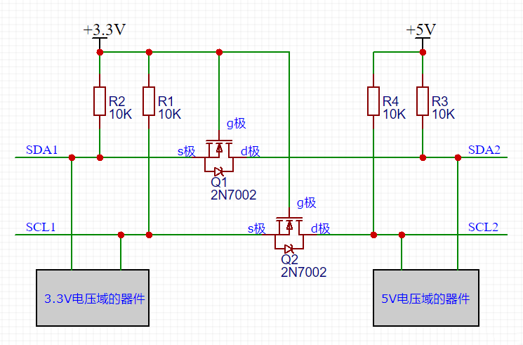
Level switch in the circuit design is very common, because of circuit design, most of the time just like in the building blocks of the circuit module, and the circuit module, patchwork together is a electronic products. However, the voltage domain is often inconsistent between modules, so the level conversion circuit is used for the communication between modules.
The figure above is an I2C bus level conversion circuit implemented by MOS tube, realizing bidirectional communication between 3.3V voltage domain and 5V voltage domain. With 3.3V and 5V devices hooked up to the bus, you can have fun and chat.
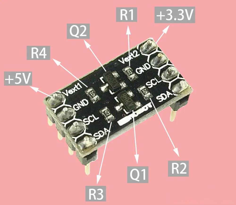
The picture of object comparison is as follows. The physical pull-up resistance USES 4.7K ohms, providing greater current drive capability. On the premise of satisfying circuit performance, I prefer to use resistors with higher resistance value, because of lower power consumption and less power consumption.

Level switch in the circuit design is very common, because of circuit design, most of the time just like in the building blocks of the circuit module, and the circuit module, patchwork together is a electronic products. However, the voltage domain is often inconsistent between modules, so the level conversion circuit is used for the communication between modules.
The figure above is an I2C bus level conversion circuit implemented by MOS tube, realizing bidirectional communication between 3.3V voltage domain and 5V voltage domain. With 3.3V and 5V devices hooked up to the bus, you can have fun and chat.
The picture of object comparison is as follows. The physical pull-up resistance USES 4.7K ohms, providing greater current drive capability. On the premise of satisfying circuit performance, I prefer to use resistors with higher resistance value, because of lower power consumption and less power consumption.
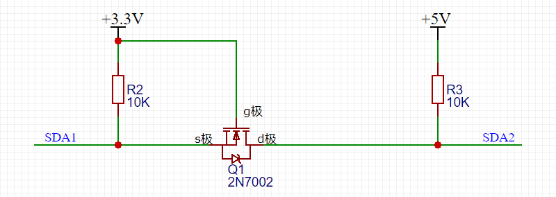
The original analysis
There are four cases:
1. When SDA1 outputs high power, VGS of MOS tube Q1 = 0, MOS tube is turned off, and SDA2 is pulled to 5V by resistor R3.
2. When SDA1 outputs low power, THE VGS of MOS tube Q1 = 3.3V, which is greater than the on-on voltage, the on-off voltage of MOS tube, and SDA2 is pulled to low level through the MOS tube.
3. When THE OUTPUT of SDA2 is high, the VGS of MOS tube Q1 remains unchanged, MOS maintains the closed state, and SDA1 is pulled up to 3.3V by resistor R2.
4, when SDA2 output low power usually: MOS tube not conduction, but it has a body diode! The volume diode in the MOS tube pulls THE SDA1 to a low level, at which time the VGS is approximately equal to 3.3V, and the MOS tube conducts, further lowering the VOLTAGE of SDA1.
Note:
Low means equal to or close to 0V.
A high level is equal to or near the supply voltage. Therefore, for devices in the voltage domain of 3.3V, the high level is equal to or close to 3.3V; A device in a 5V voltage domain whose high level is equal to or close to 5V.
For specific requirements, see how the chip's data sheet describes this limit. Common examples include a low level below 0.3 times "chip supply voltage" and a high level above 0.7 times "chip supply voltage".
That is to say, when the "chip supply voltage" is 5V, the low level is below 5 x 0.3 = 1.5V, and the high level is above 5 x 0.7 = 3.5V.
Notes:
The above is the situation between 3.3V and 5V. If the conversion between other voltage domains is used, such as between pons of voltage values such as 3.3V, 2.5V and 1.8V, attention should be paid to the VGS of the MOS tube to turn on the on-off voltage.
Too high VGS to MOS tube will cause MOS tube burn out! Too low VGS will lead to MOS tube can not open! Different types of MOS tube this parameter value is not the same!!
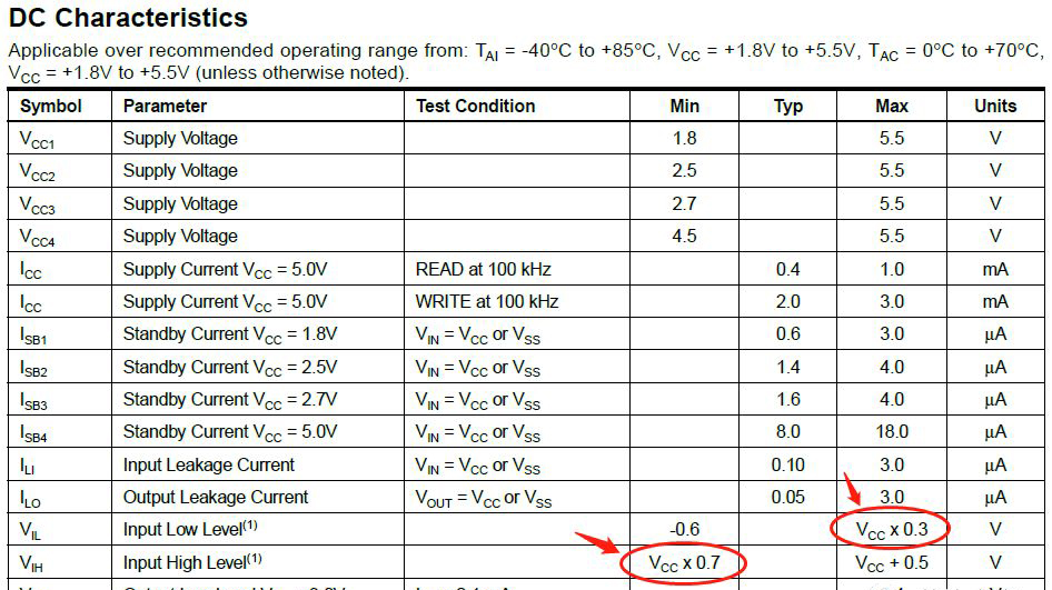
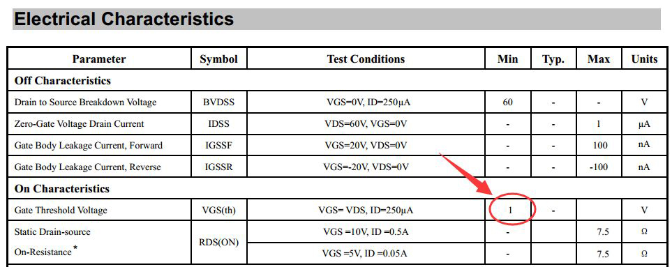
Again, the VGS may be too small when designing the circuit. The figure below is the data manual of the 2N7002:
The above is the situation between 3.3V and 5V. If the conversion between other voltage domains is used, such as between pons of voltage values such as 3.3V, 2.5V and 1.8V, attention should be paid to the VGS of the MOS tube to turn on the on-off voltage.
Too high VGS to MOS tube will cause MOS tube burn out! Too low VGS will lead to MOS tube can not open! Different types of MOS tube this parameter value is not the same!!
Again, the VGS may be too small when designing the circuit. The figure below is the data manual of the 2N7002:
In order to ensure full opening and conduction in actual use, more allowance should be reserved in design. For example, VGS in actual circuit should be at least 1.8V. Because the design parameter of 1.8V is close to the threshold value of 1V marked in the data manual, special attention should be paid to the experimental verification to ensure nothing is wrong.
Conclusion:
3.3V and 5V interrotate circuit is a classic circuit, unlike some MOS tube looks the same as 2N7002, but it is actually a high-power circuit, and some performance specifications are wasted. Some performance specifications may not meet the needs, mainly because they are expensive. I won't get into the details of other MOS.
Share


- About
- Company Profile
- Company Honor
- Products
- FIELD EFFECT TRANSISTOR
- SCHOTTKY DIODES
- ULTRAFAST RECOVERY POWER RECTIFIER
- SIC SCHOTTKY DIODES
- Silicon carbide MOSFET
- Follow
-
Address:Room 402-404,Qianhai ChengJin Building,Moon Bay Boulevard, Nanshan District,Shenzhen
Tel:0755-88327180
Fax:0755-88327190
Email:sunny@hisemicon.com
- Contact
-
.jpg)
WeChat